


C01
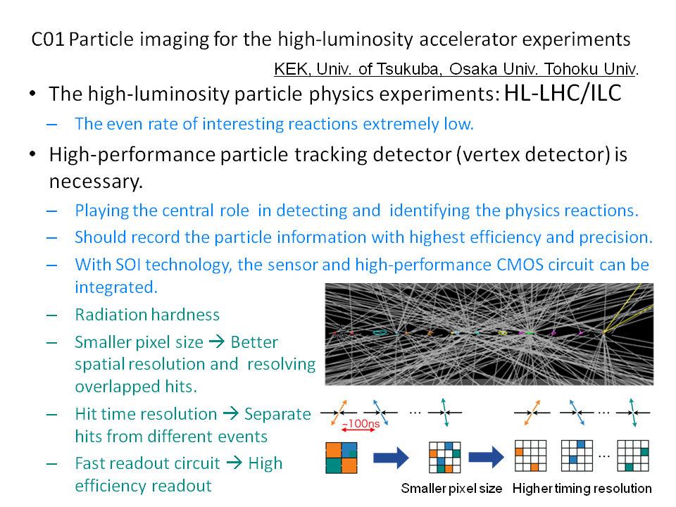
C01:Particle imaging for the high-luminosity accelerator experiments
In the proposed high-energy physics experiments, such as LHC upgrade or ILC, the rate of interesting physics phenomena is extremely low and very high luminosity particle accelerators are designed. The requirements to the vertex detector, which records the decay particles from the reaction, such as detection efficiency, spatial and timing resolution as long as the radiation hardness for long-term experiment, are increasing. The SOI technology, where the sub-micron CMOS circuit is integrated on a sensor grade silicon wafer, was chosen as the best device satisfying the above requirements. Throughout the 5-year activities, we aim to develop the high-performance SOI pixel devie and prove the performance of the device satisfies the requirements by proposed high energy experiments.
member
| Toru Tsuboyama | KEK | Experimental particle physics, Detector production and operation. | Management |
| Junji Haba | KEK | Experimental particle physics, Detector development | General device evaluation |
| Yosuke Takubo | KEK | Experimental particle physics, | High performance data acquisition system |
| Kazuhiko Hara | Tsukuba Univ. | Experimental particle physics, | Radiation hardness study |
| Akimasa Ishikawa | Tohoku Univ. | Experimental particle physics, | Device concept design and evaluation |
| Manabu Togawa | Osaka Univ. | Experimental particle physics, | Development pixel devices |
| Kazunori Hanagaki | Osaka Univ. | Experimental particle physics, Energy frontier collider experiments. | System production |
Publication
- “Observation of a new particle in the search for the Standard Model Higgs boson with the ATLAS detector at the LHC”, Physics Letters B 716 (2012) 1?29, G. Aad (K. Hanagki, K. Hara , Y.Takubo )
- “Development of SOI pixel process technology”, NIM 636, (2011), S31-S36, Y. Arai, *T. Miyoshi, Y. Unno, T. Tsuboyama, S. Terada, Y. Ikegami, R. Ichimiya, T. Kohriki, K. Tauchi, Y. Ikemoto, Y. Fujita, T. Uchida, K. Hara, et al.
- “Performance study of SOI monolithic pixel detectors for X-ray application”, NIM, 636 S237-S241(2011), *T. Miyoshi, Y. Arai, M. Hirose, R. Ichimiya, Y. Ikemoto, T. Kohriki, T. Tsuboyama, Y. Unno.
- “Radiation effects in silicon-on-insulator transistors with back-gate control method fabricated with OKI Semiconductor 0.20 μm FD-SOI technology”, *M. Kochiyama, T. Sega, K. Hara, Y. Arai, T. Miyoshi, Y. Ikegami, S. Terada, Y. Unno, K. Fukuda, M. Okihara、Nucl. Instr. and Meth. A(2010), Vol. 636, S62-S67 (2011).
- “Recent activities in HEP detector R&D”, *Junji Haba, 2010. 7pp. Published in PoS ICHEP2010:542, 2010.
- “R&D status of 64-channel photon-counting imaging module”, *Y. Kawai, J. Haba, M. Suyama, Nucl. Instr. Meth. A623 282-284 (2010).
- "Silicon vertex tracker for RHIC PHENIX experiment.", A. Taketani, *M. Togawa et al., Nucl. Instr. Meth. A623, pp.374-376, 2010.
- “Radiation Resistance of SOI Pixel Devices Fabricated With OKI 0.15 um FD-SOI Technology”, *K. Hara T. Tsuboyama et al., IEEE Trans. on Nucl. Sci., Vol. 56, 2896-2904 (2009))
- “Silicon vertex detector for Super KEK B factory”, NIM 598 (2009), 79-81, *T. Tsuboyama.
- “Development of Radiation Hard N+-on-P Silicon Micro strip Sensors for Super LHC”. *K. Hara et al., IEEE TNS, Vol.56-2, April 2009, pp468-473.
- “Development and Implementation of a Readout Module for Radiation-Sensing Field-Effect Transistors”, *Ruckman, L.; Varner, G.; Stanie, S.; Koga, A.; Tsuboyama, T.; , IEEE Trans. Nucl. Sci., 53 (2006) 2452-2455.
- “Status and perspectives of Pixelated Photon Detector (PPD).” *J. Haba, Nucl. Instr. Meth. A595:154-160, 2008.