


A02班
新着情報
記事はありません。
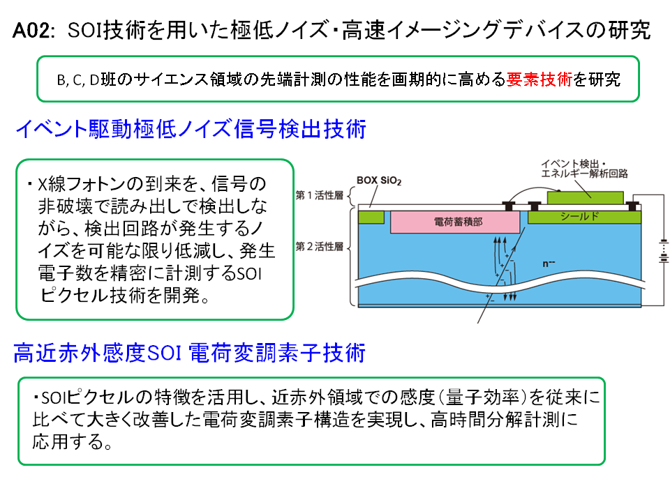
A02班:SOI技術を用いた極低ノイズ・高速イメージングデバイスの研究
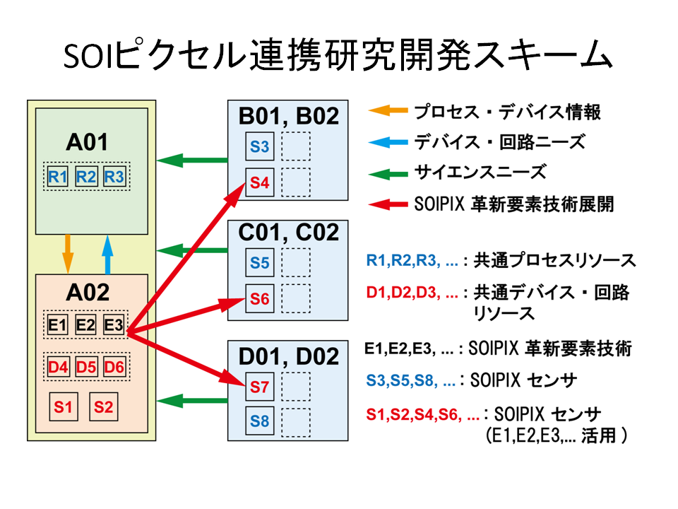
デバイスプロセスを開発するA01班と連携しながら、B, C, D班のサイエンス領域でなされる高エネルギー物理に関する先端計測を支え、その性能を画期的に高めるための要素技術について研究を行う。その中で、最も挑戦的かつインパクトの大きい技術は、イベント駆動True CDS (ET-CDS)技術である。この素子構造により、kTCノイズを完全にキャンセルできることになり、X線フォトンの入射の検出を非破壊読み出しによるイベント駆動原理により行い、かつ1電子相当の極低ノイズでのX線フォトンのエネルギー計測、すなわち超精密計測が可能となる。従来比で、1/50から1/100にノイズが低減することを目指している。
- 研究班総括 SOIピクセルセンサのデバイス・回路・アーキテクチャ設計 (川人 祥二)
- 量子検出回路の解析・設計・シミュレーション・評価 (池辺 将之)
- SOIピクセルセンサの回路設計および特性評価 (香川 景一郎)
メンバー
研究代表者:川人 祥二
静岡大電研・教授
高機能CMOS撮像素子 半導体集積回路
研究分担者:池辺 将之
北大情報・准教授
半導体集積回路
研究分担者:香川 景一郎
静岡大電研・准教授
高機能CMOS撮像素子 情報光学
研究分担者:安富啓太
静岡大電研・助教
高機能CMOS撮像素子 半導体集積回路
連携研究者:亀濱 博紀
静岡大創造・博士後期課程 低ノイズCMOS撮像素子
連携研究者:内田大輔
北大情報・博士前期課程
半導体集積回路
連携研究者:染谷槙人
北大情報・博士前期課程
半導体集積回路
連携研究者:築田聡史
北大情報・博士前期課程
半導体集積回路
リンク
静岡大学 川人研究室: http://www.idl.rie.shizuoka.ac.jp/
北海道大学 知能システム学研究室: http://impulse.ist.hokudai.ac.jp/
論文等
- M.Ikebe, "Recent progress in the technology linking sensors and digital circuits," IEICE Electronics Express, Vol. 11, No. 3 pp. 20142003 (2014).
- D.Uchida, M.Ikebe, J.Motohisa, E.Sano, and A.Kondou, "CMOS common-mode rejection filter with floating active transformer operation," Jpn. J. Appl. Phys., Vol. 53, p. 04EE20 (2014).
-
S.Kawahito, “Innovation in charge domain global shutter technologies”, Image Sensors 2014, 16.4,
pp.1-31 (London, Mar. 2014).(Invited)
-
S.Kawahito, “Low Noise High Dynamic Range CMOS Image Sensor,” SEMICON Korea 2014 (Seoul, Feb. 2014).(Invited)
-
K.Yasutomi, T.Usui, S-M.Han, T.Takasawa, K.Kagawa, S.Kawahito, “A 0.3mm-Resolution Time-of-Flight CMOS Range Imager with Column-Gating Clock-Skew Calibration”, 2014 IEEE INTERNATIONAL SOLID-STATE CIRCUITS CONFERENCE, 7.5, pp1-17 (San Francisco, Feb. 2014).
-
S-M.Han, T.Takasawa, T.Akahori, K.Yasutomi, K.Kagawa, S.Kawahito, “A413×240-Pixel Sub-Centimeter Resolution Time-of-Flight CMOS Image Sensor with In-Pixel Background Canceling Using Lateral-Electric-Field Charge Modulators”, 2014 IEEE INTERNATIONAL SOLID-STATE CIRCUITS CONFERENCE, 7.4, pp1-19 (San Francisco, Feb. 2014).
- M-W.Seo, T.Sawamoto, T.Akahori, T.Iida, T.Takasawa, K.Yasutomi, S.Kawahito, “A low noise wide dynamic range CMOS image sensor with low-noise transistors and 17b column-parallel ADCs”, IEEE Sensors Journal, Vol.13, No.8, pp2922-2929 (2013).
-
M. A. Mustafa, M-W.Seo, S.Kawahito, K.Yasutomi, K.Kagawa, “RTS Noise Reduction of CMOS Image Sensors Using Amplifier-Selection Pixels,” IEICE Electronics Express, pp1-7 (2013).
- K. Yasutomi, T. Usui, S-M. Han, M. Kodama, T. Takasawa, K. Kagawa, S. Kawahito, “A time-of-flight image sensor with sub-mm resolution using draining only modulation pixels,” Proc. Int. Image Sensor Workshop, pp. 357-360 (2013).
- S. Kawahito, G. Baek, Z. Li, S-M. H, M-W. Seo, K. Yasutomi, and K. Kagawa, “CMOS lock-in pixel image sensors with lateral electric field control for time-resolved imaging,” Proc. Int. Image Sensor Workshop, pp. 361-364 (2013).
- K. Kagawa, M-W. Seo, K. Yasutomi, S. Terakawa, and S. Kawahito, “Multi-beam confocal microscopy based on a custom image sensor with focal-plane pinhole array effect,” Optics Express, Vol. 21, Issue 2, pp. 1417-1429 (2013).
- Z. Li, S. Kawahito, K. Yasutomi, K. Kagawa, J. Ukon, M. Hashimoto, and H. Niioka, “A time-resolved CMOS image sensor with draining-only modulation pixels for fluorescence lifetime imaging,” IEEE Trans. Electron Devices, vol.59, pp.2715-2722 (2012).
- M.-W. Seo, S-H Suh, T. Iid, T. Takasawa, K. Isobe, T. Watanabe, S. Itoh, K. Yasutomi, and S. Kawahito, “A low-noise high intrascene dynamic range CMOS image sensor with a 13 to 19b variable-resolution column-parallel folding-integration/cyclic ADC,” IEEE J. Solid-State Circuits, vol. 47, pp.272-283 (2012).
- M. Ikebe and J. Motohisa, “A CMOS imager with negative feedback pixel circuits and its applications,” Proc. SPIE 8194, International Symposium on Photoelectronic Detection and Imaging: Advances in Imaging Detectors and Applications, 819402 (2011).
- K. Yasutomi, S. Itoh, and S. Kawahito, “A two-stage charge transfer active pixel CMOS image sensor with low-noise global shuttering and a dual-shuttering mode”, IEEE Trans. Electron Devices, vol.58, pp.740-747 (2011).
- S. Muung, M. Ikebe, J. Motohisa, and E. Sano, “Column parallel single-slope ADC with time to digital converter for CMOS imager,” IEEE Int'l Conf. Electronics Circuits and Systems, pp. 863-866 (2010)
- M. Ikebe and J. Motohisa, “An Intelligent CMOS Image Sensor with negative feedback resetting”, ECTI Trans. on Elec. Eng., Electronics, and Comm. Vol. 8, No. 2, pp. 217 ? 223 (2010).
- S. Muung, M. Ikebe, and J. Motohisa, and E. Sano “Column parallel single-slope ADC with time to digital converter for CMOS imager,” IEEE Int'l Conf. Electronics Circuits and Systems, pp. 863-866 (2010).