


A02-Ⅰ
新着情報
記事はありません。
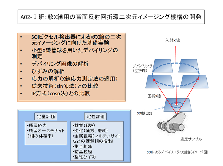
A02-1班:軟X線用の背面反射回折環二次元イメージング機構の開発
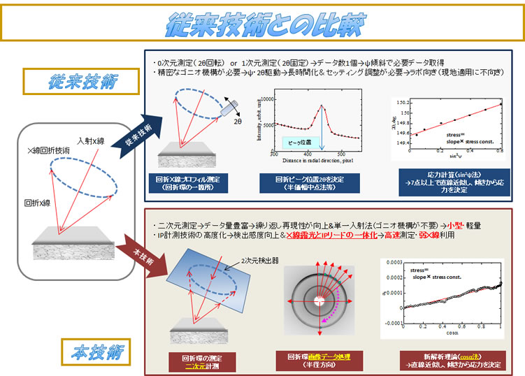
本研究は、SOI技術の応用の一つであり、機械金属部品や構造物の製造過程や保守検査に利用するものである。これらの測定対象は、微細な結晶粒の集合体からできていることが多く、X線を当てるとデバイリングと呼ばれる円環状のX線を発生させる(X線回折現象)。このようなX線回折ビームを計測すると、測定部の残留応力や結晶組織の状態が種々判明し、品質の判断や耐久性の評価に役立つ。従来からX線回折法やX線応力測定法として古くから利用されてきた技術であるが、計測時間や小型化の制約があったため、ラボでの使用に止まることが多かった。SOI技術によれば、デバイリングの2次元情報を有効に利用できるので、高速で小型軽量な装置が実現し、これまでは利用することが困難とされてきた製造ラインでの全数検査や屋外の実機などに適用できることが期待される。本研究は、そのような装置の心臓部となるSOI検出器の開発を目指すものである。
メンバー
研究代表者:佐々木 敏彦
金沢大学人間社会研究域人間科学系・教授
研究のとりまとめ
研究協力者:江尻 正一
岩手医科大学 教養教育センター 情報科学科・教授
X線応力解析理論
研究協力者:鷹合 滋樹
石川県工業試験場 機械金属部 専門研究員
材料強度
研究協力者:幸田啓
独立行政法人 高齢・障害・求職者雇用支援機構
ポリテクカレッジ千葉 電子情報技術科
X線装置、制御回路
・論文等
・ T. Miyazaki and T. Sasaki, X-ray stress measurement with two-dimensional detector based on Fourier analysis, Int. J. Mater. Res. (formerly Z. Metallkd.), 105(2014) to be published.
・矢口修、宮崎利行、佐々木敏彦, 渦電流法による鋳造カムシャフトのチル化率評価, 非破壊検査, vol.64, No.7 (2014) 掲載予定.
・T.Sasaki, Y.Maruyama, H.Ohba and S.Ejiri, Two-Dimensional Imaging of Debye-Scherrer Ring for Tri-axial Stress Analysis of Industrial Materials, The Journal of Instrumentation (2014) to be published.
・T.Sasaki, New Generation X-Ray Stress Measurement Using Debye Ring Image Data by Two-Dimensional Detection, Materials Science Forum Vols. 783-786 (2014) pp 2103-2108.
・T. Sasaki, T. Miyazaki, H. Ito, T. Furukawa and T. Mihara, X-ray Residual Stress Analysis of Nickel Base Alloys, Advanced Materials Research Vol. 922 (2014) pp 274-279.
・Determination of Shearing Stresses (τxz and τyz) Using X-ray Diffraction Method with Two-Dimensional Detector, T.Sasaki, J.Akita, Y.Sone and Y.Kobayashi、Materials Science Forum、Vols.706-709, pp.1719-172(2012) ,
・Indentification of Iron Rusts on Rail by X-ray Diffraction and Vibrational Analysis, Y.Sone, J.Suzumura, N.Kamura and T.Sasaki, Advanced Materials Research, Vol.409, pp.581-585(2012),
・高橋俊一、加藤孝憲、鈴木裕士、佐々木敏彦, 鉄道用車輪の残留応力評価,日本機械学会論文集A、第76巻、第763号、pp.283~289、(2010)
・佐々木敏彦、高橋俊一、佐々木勝成、小林裕一,エリアディテクタ方式のX線三軸応力測定法の改良に関する研究,日本機械学会論 文集A、第71巻、第704号、pp.670~676、(2009)
論文等
- M.Ikebe, "Recent progress in the technology linking sensors and digital circuits," IEICE Electronics Express, Vol. 11, No. 3 pp. 20142003 (2014).
- D.Uchida, M.Ikebe, J.Motohisa, E.Sano, and A.Kondou, "CMOS common-mode rejection filter with floating active transformer operation," Jpn. J. Appl. Phys., Vol. 53, p. 04EE20 (2014).
-
S.Kawahito, “Innovation in charge domain global shutter technologies”, Image Sensors 2014, 16.4,
pp.1-31 (London, Mar. 2014).(Invited)
-
S.Kawahito, “Low Noise High Dynamic Range CMOS Image Sensor,” SEMICON Korea 2014 (Seoul, Feb. 2014).(Invited)
-
K.Yasutomi, T.Usui, S-M.Han, T.Takasawa, K.Kagawa, S.Kawahito, “A 0.3mm-Resolution Time-of-Flight CMOS Range Imager with Column-Gating Clock-Skew Calibration”, 2014 IEEE INTERNATIONAL SOLID-STATE CIRCUITS CONFERENCE, 7.5, pp1-17 (San Francisco, Feb. 2014).
-
S-M.Han, T.Takasawa, T.Akahori, K.Yasutomi, K.Kagawa, S.Kawahito, “A413×240-Pixel Sub-Centimeter Resolution Time-of-Flight CMOS Image Sensor with In-Pixel Background Canceling Using Lateral-Electric-Field Charge Modulators”, 2014 IEEE INTERNATIONAL SOLID-STATE CIRCUITS CONFERENCE, 7.4, pp1-19 (San Francisco, Feb. 2014).
- M-W.Seo, T.Sawamoto, T.Akahori, T.Iida, T.Takasawa, K.Yasutomi, S.Kawahito, “A low noise wide dynamic range CMOS image sensor with low-noise transistors and 17b column-parallel ADCs”, IEEE Sensors Journal, Vol.13, No.8, pp2922-2929 (2013).
-
M. A. Mustafa, M-W.Seo, S.Kawahito, K.Yasutomi, K.Kagawa, “RTS Noise Reduction of CMOS Image Sensors Using Amplifier-Selection Pixels,” IEICE Electronics Express, pp1-7 (2013).
- K. Yasutomi, T. Usui, S-M. Han, M. Kodama, T. Takasawa, K. Kagawa, S. Kawahito, “A time-of-flight image sensor with sub-mm resolution using draining only modulation pixels,” Proc. Int. Image Sensor Workshop, pp. 357-360 (2013).
- S. Kawahito, G. Baek, Z. Li, S-M. H, M-W. Seo, K. Yasutomi, and K. Kagawa, “CMOS lock-in pixel image sensors with lateral electric field control for time-resolved imaging,” Proc. Int. Image Sensor Workshop, pp. 361-364 (2013).
- K. Kagawa, M-W. Seo, K. Yasutomi, S. Terakawa, and S. Kawahito, “Multi-beam confocal microscopy based on a custom image sensor with focal-plane pinhole array effect,” Optics Express, Vol. 21, Issue 2, pp. 1417-1429 (2013).
- Z. Li, S. Kawahito, K. Yasutomi, K. Kagawa, J. Ukon, M. Hashimoto, and H. Niioka, “A time-resolved CMOS image sensor with draining-only modulation pixels for fluorescence lifetime imaging,” IEEE Trans. Electron Devices, vol.59, pp.2715-2722 (2012).
- M.-W. Seo, S-H Suh, T. Iid, T. Takasawa, K. Isobe, T. Watanabe, S. Itoh, K. Yasutomi, and S. Kawahito, “A low-noise high intrascene dynamic range CMOS image sensor with a 13 to 19b variable-resolution column-parallel folding-integration/cyclic ADC,” IEEE J. Solid-State Circuits, vol. 47, pp.272-283 (2012).
- M. Ikebe and J. Motohisa, “A CMOS imager with negative feedback pixel circuits and its applications,” Proc. SPIE 8194, International Symposium on Photoelectronic Detection and Imaging: Advances in Imaging Detectors and Applications, 819402 (2011).
- K. Yasutomi, S. Itoh, and S. Kawahito, “A two-stage charge transfer active pixel CMOS image sensor with low-noise global shuttering and a dual-shuttering mode”, IEEE Trans. Electron Devices, vol.58, pp.740-747 (2011).
- S. Muung, M. Ikebe, J. Motohisa, and E. Sano, “Column parallel single-slope ADC with time to digital converter for CMOS imager,” IEEE Int'l Conf. Electronics Circuits and Systems, pp. 863-866 (2010)
- M. Ikebe and J. Motohisa, “An Intelligent CMOS Image Sensor with negative feedback resetting”, ECTI Trans. on Elec. Eng., Electronics, and Comm. Vol. 8, No. 2, pp. 217 ? 223 (2010).
- S. Muung, M. Ikebe, and J. Motohisa, and E. Sano “Column parallel single-slope ADC with time to digital converter for CMOS imager,” IEEE Int'l Conf. Electronics Circuits and Systems, pp. 863-866 (2010).