FY21-1 KEK/Lapis 0.20um SOI CMOS Pixel MPW run (MX2263)
Last updat Mar 16, 2023
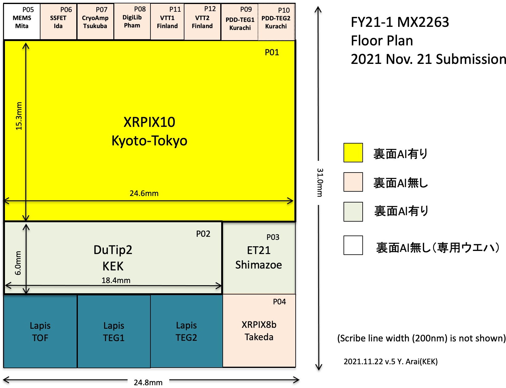
Floore Plan
What's New
- Mar. 16, 2023: Lapis Semitools License is updated. (see --> PDK)

- July 12, 2022: SOIPIX standard process flow document is prepared. (see --> Other Documents)
- Mar. 31, 2022: Lapis Semitools License is updated. (see --> PDK)
- Aug. 3, 2021: This page is created.
- July 30, 2021: PDK supporting 3D integration (Rel.0518) is released. (see --> PDK)
- Mar. 31, 2021: Lapis Semitools License is updated. (see --> PDK)
- Dec. 1, 2020: New PDK Rel.0516 is released. (see --> PDK)
- Nov. 24, 2020: Drawing rule document is updated to Rev32. (see --> PDK)
- Nov. 20, 2020: 1.8V I/O library is updated to v.1. (see --> Cell Lib)
- Nov. 16, 2020: New DRC rule which correct false 'VP' errors in AC merg regio is released. (see --> PDK)
- Nov. 16, 2020: Release note of the1.8V I/O library is revised. (see --> Cell Lib)
- Oct. 16, 2020: If you get 'POLY_W1' DRC errors, please remove comment out mark '#' from line 23 'POLY pin 118 0' in the PC_020umSOI_KEK/PC_020umSOI_KEK.layermap file.
- Sep. 11, 2020: Drawing Rule Rev.29 & PDK Rel.05.13 is released. (see --> PDK)
- Sep.11, 2020: PDD Design Guide V.08 is released. (see --> TIPS)
- Sep. 2, 2020: 1.8V I/O Library developed at KEK is released. (see --> Cell Lib)
Deadline of expression of interest : July 31, 2021
Fix submission, mask area and cost: Aug. 31, 2021
Deadline of submission : Nov. 21, 2021
finish wafer process : end of Mar. 2022.
finish backside process and dicing : end of May 2022.
Scheduled delivery of chips : beginning of June.
Submission
- 1) Please put chip ID Mark on your chip. (see --> Cell Lib)
- 2) Please set origin of your chip at the CENTER of your chip.
- 3) If you want to trace wafer No. and chip location in the wafer, please put 20 bits fuse (ltfuse_20) on your chip. (see --> PDK)
- 4) Please put Outer Frame (GDS#64=OF) according to the 7.9 of the Drawing Rule. (from this run, check of Outer frame existence is added to the DRC rule. You can neglect this DRC error except at top cell.)
- 5) Please name top cell name as 'top_id_name'. For exampl, if your Chip ID is 'JK1' and chip name is 'INT4', top cell name of your chip should be 'top_JK1_INT4' ('top' must be small character!!!).
Send following files to Yasuo Arai (yasuo.arai@kek.jp) via e-mail or through internet server;
- a) Submission Check Sheet.
- b) GDS file.
- c) DRC summary file (top_xxxx.drc.summary) and result file (top_xxxx.drc.results)
=== Notes on this MPW run ===
- In this MPW run, default substrate is p-type and thickness of BOX is 145 nm. Pinned Depleted Diode (PDD) structure can be used. Threre are a plan for 3D integration but no plan for double SOI.
- GDS #53 is named as BN5 for PDD BNW2 layer.
- Until MX2199 run, polarity of dopants was reversed for p-type substrate (for example, BPW means n-type buried layer in p-substrate). In this run, the BPW layer means p-type buried layer for both n-type and p-type substrates.
So, please be careful if you intend to use old cell design.
- New IO library ‘IOLIBP1’ is prepared for p-type substrate. (If you design chip for n-type substrate, then please keep using previous IO library ‘IOLIB6’.)

- Doping density of LDD region of transistors is increased from MX2040 run to improve radiation hardness and low temperature characteristics.
LDD doping node of PMOS becomes 6 times higher, and that of NMOS becomes 2.5 times higher.
- Due to this change, transistor characteristics are changed. SPICE model supplied from Lapis does not include this change. Instead, you can use SPICE models extracted by Modech Co. Ltd. Modech LDD SPICE model .
- 45 degree routing of metal layer is possible, but it must be converted to polygon from path and the cordinate must be on grid. Also be caful that the width of the metal fulfills DRC rule at everywhere.
- This run is 5 metal process (use rule files of '..._5m_...').
- Location of MIM Capacitor is between M3 and M4 and use 'mimcap_1p5f' cell. Thick metal of M5 may be good to use for power/gnd lines.
- You can create round corner. Use 'Create Polygon' -> 'Create Arc' command in Virtuosso.
- Dummy metals will be generated by Lapis. If you don't want to put dummy metals, please use no dummy matel layer (#96~100).
PDK
-
Mar. 16, 2023: New SOI SemiTOOLS of which license is extended to Mar. 31, 2024 are released. LAPIS_Semi_TOOLS61_Setup_Guide_English.pdf, LAPIS_Semi_TOOLS61_STL_v13_20240331.tar.gz
(You can check the expiration date by enterring 'LMshowtimelimit' in the CIW window.)
-
Mar. 31, 2022: New SOI SemiTOOLS of which license is extended to Mar. 31, 2023 are released.LAPIS_Semi_TOOLS61_Setup_Guide_English.pdf, LAPIS_Semi_TOOLS61_STL_v13_20230331.tar.gz
- July 30, 2021: PDK supporting 3D integration (Rel.0518) is released. (RelNote_0518, Spec_V1.00, soi020_kek_LAPIS_Semi_ic61_REL0518.tar.gz)
- Dec. 1, 2020: New PDK Rel.0516 is released. (Rel. note, soi020_kek_LAPIS_Semi_ic61_REL0516.tar.gz
- Nov. 24, 2020: Drawing Rule document is updated (Rev. 32.0) . 'non AC dummy (NDAC)' (GDS#115) and 'AC Dummey (DAC)'(GDS#113) layers are added.
- Nov. 16, 2020: New DRC rule '020soi_for_KEK_calibre_drc_5m_r31_1.rule' is released. False DRC 'VP' errors occured in Active merge region are amended.(line94 include "CTEXT" is commented out!)
- Sep. 11, 2020: Drawing Rule Rev. 29 is released.
- Sep. 11, 2020: PDK Rel. 0513_ic61 is released. (Rel. Note, PDK Rel_0513)
- Mar. 22, 2017: 20 bit fuse (manual, gds). If you want to trace wafer number and your chip location within wafer, please put this fuse pattern on your chip in vertical direction.
- Apr. 25, 2016 : Documents in PDK Rel. 0510_ic61 (Documents) not included in Rel.0513.
- Sep. 10, 2014 : 1/f model parameters are updated. Please replace relevant files in 02_soi020_kek_LAPIS_Semi_ic61/SIM_PARAM/hspice/Core directory with this.
Other Documents
- July 12, 2022: SOIPIX standard process flow document (FWP-305617 v.2)
- June 5. 2013 : SPICE Simulation Parameters (QSD-11523, Rev. 11)
- June 3, 2013 : Hot Carrier Reliability Standard (QSD-11041, Rev. 4)(English)
- June 1, 2010 : Electro Migration Standard (QSD-10606, v. 3)(Japanese, English)(recommendation)
- Jan. 29, 2010 : Guideline for Dummy Metal Prohibit Area (Japanese, English)
- July 7, 2009 : Summary Report on Sensor Diode and BPW layer (09HAC-1259_FS2Y0-001JA with English Translation)
- Jan. 26, 2009 : Calibre CCI RC extraction User's Guide (pdf(Japanese, English), Query_command_template, Star_command_template))
SPICE
- May 24, 2018: New Nch LVt model by Modech is released which improve transient analysis conversion (Document, 02soi_3p3v_nch_colvbf.inc)
- Sep. 27, 2017 : There was an error in 1/f noise model of nch_convst2 in previous Modech model. Please replace to new one. New Modech SPICE models for the increased LDD. Extracted 1/f noise models are only for nth and pct of ionvst2, colvst2, convst2, convbf. For other transistors, SPICE default model may be used.
- June 14, 2016 : SPICE model of core diode written by A-R-Tec.
- June 25, 2012 : SPICE rev.8 readme.txt (English), readme_core_st_lv_e.txt (English)
- June 30, 2009 : How to specify Body-Tie, Source-Tie, and Body-Floating Tr parameters in SPICE (pdf)
- June 23, 2009 : Diode model of dio_ppn_io is only supported (Layout & I-V curve)
User Cell Libraries
(Please use these at your own risk.)
- Nov. 20, 2020: 1.8V I/O Library developed at KEK is updated (IOLIBP1_1P8_v1.tar.gz). (No dummy metal layers in the ioAOBUF18EN3_5M4_RR_VF cell are extended to uppper region). Please define this library as 'IOLIBP1_1P8' in cds.lib.
- Nov. 6, 2020: Release note of the 1.8V I/O lib is revised.
- Dec. 5, 2018: Arai's private I/O library. New IOlib for p-type substrate IOLIBP1_v1 (readme, IOLIBP1_v1b.tar.gz)
- Oct. 1, 2017: Arai's private D-type Flip/Flop library with PMOS-NMOS active merge. (DFFLIB V.2 manual, library)
- Apr. 28, 2016: Digital Library designed by Sebastian Glab (AGH, Krakow) (Cell List, DigiLib_20120929)
- Mar. 13, 2015 : SRAM Cell designed by I. Kurachi (Manual, 48bit_array, dualport_64bit_array, Whole Library)
- Sep. 28, 2014 : Please put an ID mark characters like 'LK1' to your chip to identify your chip visually. Your chip ID will be assigned soon.
The letter should be written by using Metal 5, and preferably placed on upper right corner. Recommended height of the letter is 40 um or more. Examples (gif, gds(included in IOLIBP1))
- Oct. 7, 2019 : LVDS Driver/Receiver Data Sheet (1108LVDSspec_v2 )
- July 16, 2010 : Lapis I/O Buffer and Power/GND cell Release Note (Japanese, English) . Layouts and data sheets are included in the PDK Documents.
Packaging
Please use following Pad-Pin Wiring assignment as much as possible if you want standard packaging.
- 2.9x2.9 mm2 chip (PGA176, ioring29L2_5M5, 92+4 pads)
- 2.9x2.9 mm2 chip (PGA176, ioring29_5M5, 108+4 pads)
- 4.45 x 4.45 mm2 chip (PGA176, ioring45L2_5M5, 152+4 pads)
- 4.45 x 4.45 mm2 chip (PGA176, ioring45_5M5, 168+4 pads)
- 6.0x6.0 mm2 chip (PGA176, ioring60L2S_5M5, 176pin/184+4 pads)
- 6.0x6.0 mm2 chip (PGA240, ioring60L2_5M5, 216+4 pads, v5b)
- 6.0x6.0 mm2 chip (PGA240, ioring60_5M5, 232 pads, v5b)
Design Tips (by Y.Arai)
- Nov. 18, 2020: DRC & LVS option rule files which check detector part etc. made by Maciej Kachel (iphc.cnrs.fr) (readme, DRC, LVS)
- Nov. 18, 2020: LVS option rule files by Shun Ono (LVS)
- Sep. 11, 2020: PDD Structure Layout Guideline (v.08)
- Jan. 23, 2019 : How to add additional layers to Lapis technology file and Library for PDD design (020techfile_replace.txt, 020soi_kek_arai0510b.tech, display_arai0510b.drf, PC_020umSOI_KEK_arai.layermap)
- Dec. 20, 2018: Threshold shift dependence on Back-gate bias by Kurachi.
- Apr. 28, 2016 : Calibre PEX (Parasitic EXtraction). Rule files are exist in (work dir)/rules/xrc. Document and calview.cellmap file prepared by Ikebe san. Arai's files (calibre_pex.runset, calibre_pex_option.rul).
- Apr. 22, 2016 : An example of SPICE include files (1603selectR0509_typ.inc)
- Apr. 5, 2016 : Comparison of measurement and simulation in Ron and Ioff of Pass Tr logics (pdf).
- Oct. 14, 2014 : Role of IMB Mask layer (pdf).
- Oct. 14, 2014 : Calibre LVS : Method to remove errors for Lapis resistors (pdf)
- Oct. 8, 2014 : To reduce leakage current of transistors @Vg=0, set '.option gmindc=1e-24 gmin=1e-24' in SPICE abd use this model.
- Aug. 1, 2014: SOI Design Lecture Slides (Install, Schematics, Layout, Tips)
- Aug. 1, 2014 : Calibre files (calibre_lvs_option.rul, calibre_lvs.runset, calibre_drc_option.rul, calibre_drc.runset, calibre_antena_drc_5lmG.runset, calibre_antena_drc_5lmSD.runset, calibre_drc_Marea.runset, calibre_drc_logicgen.runset, calibre_drc_gencheck.runset). Please edit to use your directory and latest rule files.
- Aug. 1, 2014 : An example of a simple pixel (Simple_PIX.tar.gz)
- Dec. 29, 2013 : To check the PDK License time limit, enter 'LMshowtimelimit' in the Virtuoso CIW window.
- Dec. 4, 2012 : How to convert IC5.1 library to IC6.1 library (pdf).
- June 15, 2012 : If you get "WARNING: Invalid PATHCHK request "! POWER": no POWER nets present, operation aborted." in LVS, please add your Power(Gronud) name in the LVS rule file or LVS option file as "LVS POWER NAME myvdd". New option file 'calibre_lvs_option.rul' is available. Set LVS Report Option 'A B C D E' to skip Resistor w & l check.
- May 24, 2012 : An example of pixel layout (fpix1) (pdf, fpix.gds.gz)
------
Price List
* MPW run Base Price (22 bare chips)
2,800 kYen/2.9x2.9 mm2 chip
5.300 kYen/4.45x4.45 mm2 chip
8,800 kYen/6.0x6.0 mm2 chip
Other size: negotiable
***
Academic user can receive 30%~50% discount from above prices. The discount rate will depend on total requested chip area and budget joining this MPW run. You may be able to get more chips in case less than 50% discount where we duplicate chip design in a mask to fulfill the mask area.
***
* Additional chips (22 bare chips) from different wafer in the MPW run
250 kYen/2.9x2.9 mm2 chip
500 kYen/6.0x6.0 mm2 chip
Other size: negotiable
* Cost for Packaging
under negotiation
* Additional Wafer run for a single user (temprally)
'1,300 kYen(process+wafer)' /wafer for HR1(CZn) wafer
'1,320 kYen(process) + 71.5 kYen(wafer)' /wafer for FZn wafer
'1,420 kYen(process) + 150 kYen(wafer)' /wafer for Doubel-SOI wafer
For Japanese user : Consumption Tax will be added to above price.
For Overseas user : Handled by H-REPIC Co. Ltd. Shipping and handling fee will be added to above price.
Mailing List
- Please use our mailing list "soicad@ml.post.kek.jp" (for designer) or "soipix@ml.post.kek.jp" (for all collaborator) for your questions and comments.
- Mailing list help is available by sending a mail which containn 'help' in mail text to "soicad-ctl@ml.post.kek.jp".
- You can get past mail index by sending 'index', and get the mail by sending 'get xxx(index number)' to "soicad-ctl@ml.post.kek.jp"
Useful References
If you find any problem in this page, please contact to takeda@astro.miyazaki-u.ac.jp or yasuo.arai@kek.jp