


A02
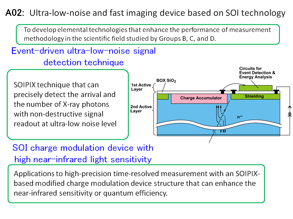
A02:Ultra-low-noise and fast imaging device based on SOI technology
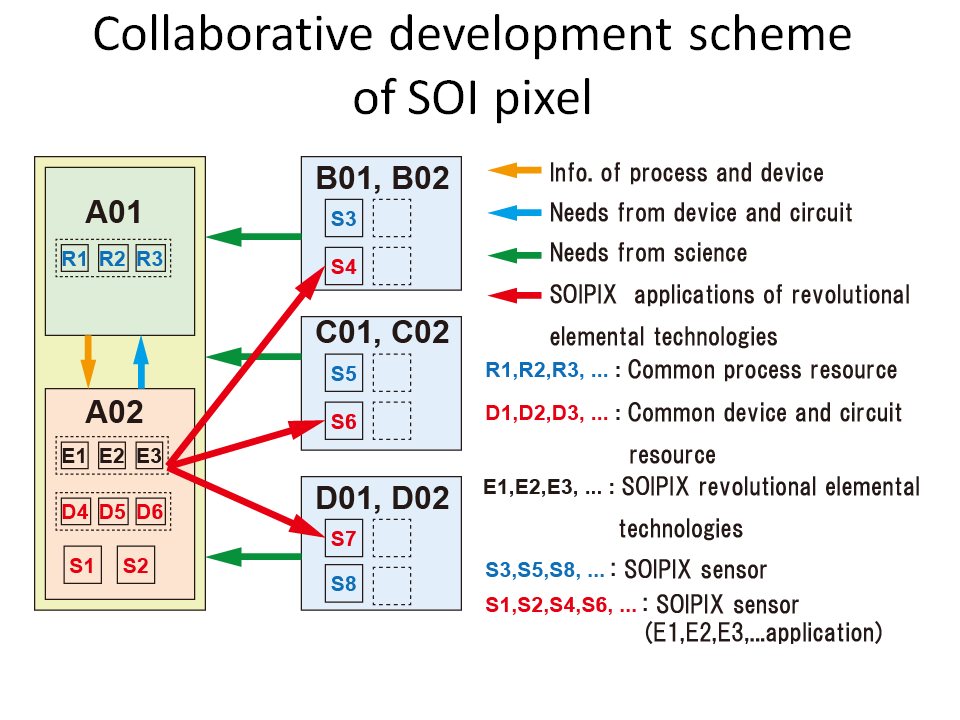
We are supporting cutting-edge measurement methodology in high-energy physics to be studied in Groups B, C, and D in cooperation with Group A01 that develops the device process, and developing elemental technologies that will significantly improve its performance. The most ambitious and essential technology is an event-driven “True CDS (ET-CDS)” technique, which will completely eliminate the kTC noise, and will realize non-destructive X-ray photon detection with an event-driven principle and ultra-low-noise precise X-ray energy measurement at one electron noise level. Compared with conventional noise levels, noise reduction of 1/50 to 1/100 is projected.
- Device, circuits, and architecture design of SOI pixel sensor (Shoji Kawahito)
- Analysis, design, and simulation of quantum detection circuits (Masayuki Ikebe)
- Circuit design and evaluation of SOI pixel sensor (Keiichiro Kagawa)
members
P-I:Shoji Kawahito, Professor,
Research Institute of Electronics, Shizuoka University, highly-functional CMOS imager, semiconductor integrated circuits
Co-I:Masayuki Ikebe, Associate Professor,
Graduate School of Information Science and Technology, Hokkaido University, semiconductor integrated circuits
Co-I:Keiichiro Kagawa, Associate Professor,
Research Insitute of Electronics, Shizuoka University, highly-functional CMOS imager, information photics
Cooperating Researcher:Keita Yasutomi,
Research Institute of Electronics, Shizuoka University, highly-functional CMOS imager, semiconductor integrated circuits
Cooperating Researcher:Hiroki Kamehama,
Doctor Course Student, Shizuoka University, low-noise CMOS imager
Cooperating Researcher:Daisuke Uchida,
Master Course Student, Hokkaido University, semiconductor integrated circuits
Cooperating Researcher:Makito Someya,
Master Course Student, Hokkaido University, semiconductor integrated circuits
Cooperating Researcher:Satoshi Tuzuki,
Master Course Student, Hokkaido University, semiconductor integrated circuits
Links
Imaging Device Laboratory, Shizuoka University: http://www.idl.rie.shizuoka.ac.jp/
Intelligent LSI Systems Laboratory, Hokkaido University: http://impulse.ist.hokudai.ac.jp/
Publication
- M.Ikebe, "Recent progress in the technology linking sensors and digital circuits," IEICE Electronics Express, Vol. 11, No. 3 pp. 20142003 (2014).
- D.Uchida, M.Ikebe, J.Motohisa, E.Sano, and A.Kondou, "CMOS common-mode rejection filter with floating active transformer operation," Jpn. J. Appl. Phys., Vol. 53, p. 04EE20 (2014).
-
S.Kawahito, “Innovation in charge domain global shutter technologies”, Image Sensors 2014, 16.4,
pp.1-31 (London, Mar. 2014).(Invited)
-
S.Kawahito, “Low Noise High Dynamic Range CMOS Image Sensor,” SEMICON Korea 2014 (Seoul, Feb. 2014).(Invited)
-
K.Yasutomi, T.Usui, S-M.Han, T.Takasawa, K.Kagawa, S.Kawahito, “A 0.3mm-Resolution Time-of-Flight CMOS Range Imager with Column-Gating Clock-Skew Calibration”, 2014 IEEE INTERNATIONAL SOLID-STATE CIRCUITS CONFERENCE, 7.5, pp1-17 (San Francisco, Feb. 2014).
-
S-M.Han, T.Takasawa, T.Akahori, K.Yasutomi, K.Kagawa, S.Kawahito, “A413×240-Pixel Sub-Centimeter Resolution Time-of-Flight CMOS Image Sensor with In-Pixel Background Canceling Using Lateral-Electric-Field Charge Modulators”, 2014 IEEE INTERNATIONAL SOLID-STATE CIRCUITS CONFERENCE, 7.4, pp1-19 (San Francisco, Feb. 2014).
- M-W.Seo, T.Sawamoto, T.Akahori, T.Iida, T.Takasawa, K.Yasutomi, S.Kawahito, “A low noise wide dynamic range CMOS image sensor with low-noise transistors and 17b column-parallel ADCs”, IEEE Sensors Journal, Vol.13, No.8, pp2922-2929 (2013).
-
M. A. Mustafa, M-W.Seo, S.Kawahito, K.Yasutomi, K.Kagawa, “RTS Noise Reduction of CMOS Image Sensors Using Amplifier-Selection Pixels,” IEICE Electronics Express, pp1-7 (2013).
- K. Yasutomi, T. Usui, S-M. Han, M. Kodama, T. Takasawa, K. Kagawa, S. Kawahito, “A time-of-flight image sensor with sub-mm resolution using draining only modulation pixels,” Proc. Int. Image Sensor Workshop, pp. 357-360 (2013).
- S. Kawahito, G. Baek, Z. Li, S-M. H, M-W. Seo, K. Yasutomi, and K. Kagawa, “CMOS lock-in pixel image sensors with lateral electric field control for time-resolved imaging,” Proc. Int. Image Sensor Workshop, pp. 361-364 (2013).
- K. Kagawa, M-W. Seo, K. Yasutomi, S. Terakawa, and S. Kawahito, “Multi-beam confocal microscopy based on a custom image sensor with focal-plane pinhole array effect,” Optics Express, Vol. 21, Issue 2, pp. 1417-1429 (2013).
- Z. Li, S. Kawahito, K. Yasutomi, K. Kagawa, J. Ukon, M. Hashimoto, and H. Niioka, “A time-resolved CMOS image sensor with draining-only modulation pixels for fluorescence lifetime imaging,” IEEE Trans. Electron Devices, vol.59, pp.2715-2722 (2012).
- M.-W. Seo, S-H Suh, T. Iid, T. Takasawa, K. Isobe, T. Watanabe, S. Itoh, K. Yasutomi, and S. Kawahito, “A low-noise high intrascene dynamic range CMOS image sensor with a 13 to 19b variable-resolution column-parallel folding-integration/cyclic ADC,” IEEE J. Solid-State Circuits, vol. 47, pp.272-283 (2012).
- M. Ikebe and J. Motohisa, “A CMOS imager with negative feedback pixel circuits and its applications,” Proc. SPIE 8194, International Symposium on Photoelectronic Detection and Imaging: Advances in Imaging Detectors and Applications, 819402 (2011).
- K. Yasutomi, S. Itoh, and S. Kawahito, “A two-stage charge transfer active pixel CMOS image sensor with low-noise global shuttering and a dual-shuttering mode”, IEEE Trans. Electron Devices, vol.58, pp.740-747 (2011).
- S. Muung, M. Ikebe, J. Motohisa, and E. Sano, “Column parallel single-slope ADC with time to digital converter for CMOS imager,” IEEE Int'l Conf. Electronics Circuits and Systems, pp. 863-866 (2010)
- M. Ikebe and J. Motohisa, “An Intelligent CMOS Image Sensor with negative feedback resetting”, ECTI Trans. on Elec. Eng., Electronics, and Comm. Vol. 8, No. 2, pp. 217 ? 223 (2010).
- S. Muung, M. Ikebe, and J. Motohisa, and E. Sano “Column parallel single-slope ADC with time to digital converter for CMOS imager,” IEEE Int'l Conf. Electronics Circuits and Systems, pp. 863-866 (2010).