


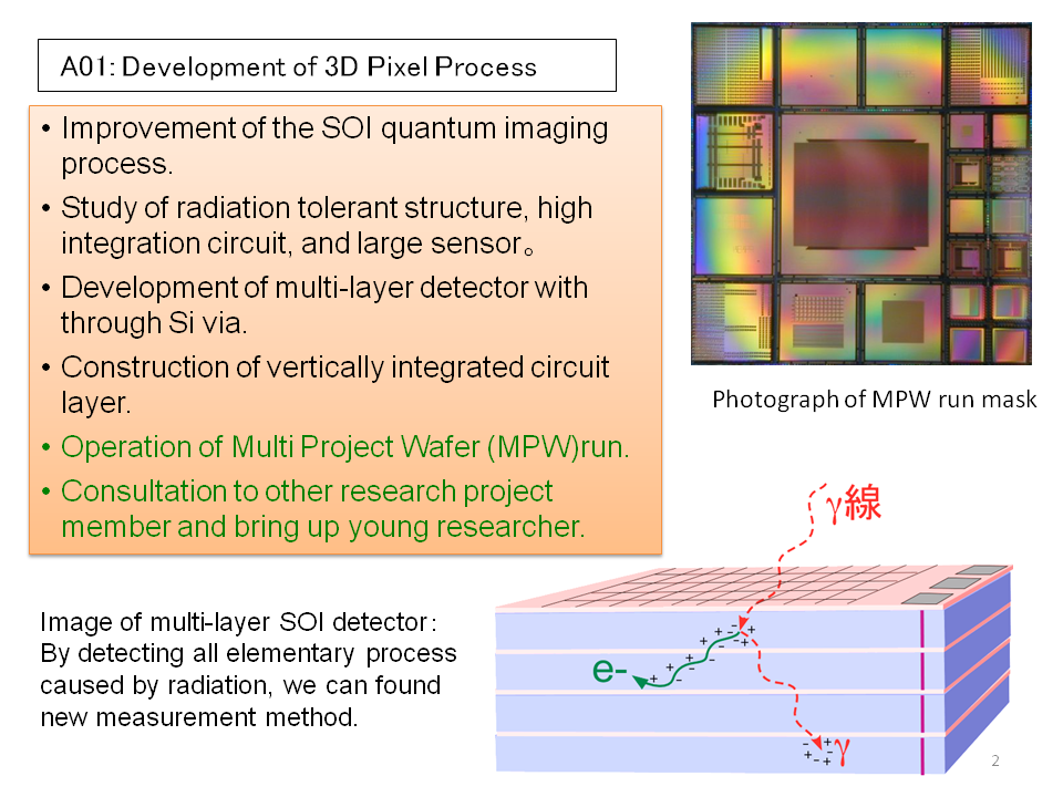
A01
A01: Development of 3D Pixel Process
This sub project is a core of this research project area. Based on the Silicon-On-Insulator (SOI) technology, we unify both radiation sensor and LSI circuit in a single chip, then develop semiconductor process for new quantum imaging detectors. We also operate regular Multi Project Wafer (MPW) run, so that other sub project group can easily build their own detectors. In addition, by using new technology such as Through Silicon Via (TSV) and vertical (3D) integration, we are aiming to develop technologies for high performance and high-resolution pixel detectors.
members
研究代表:新井 康夫
高エネルギー加速器研究機構、素粒子原子核研究所
教授
高エネルギー物理実験
理学博士
研究取りまとめ
http://research.kek.jp/people/araiy/
研究分担者:三好 敏喜
高エネルギー加速器研究機構、素粒子原子核研究所
助教
高エネルギー物理実験
理学博士
プロセス試作
研究分担者:井田 次郎
金沢工業大学、工学部
教授
電子デバイス・集積回路
工学博士
プロセス評価
http://j-ida.kit.labos.ac/ja
その他メンバー
瀧 久幸
金沢工業大学、工学部
学部4年 (大学院進学予定)
Publication
- Y. Arai,“Advanced Radiation Image Sensors with SOI technology”, *Y. Arai, 2012 International Conference on Solid State Devices and Materials (SSDM 2012), Sep. 25-27, 2012, Kyoto International Conference Center, Kyoto, Japan. Proceedings, J-1-1, pp. 1107-1108.[招待講演]
- Ryo Umesao, Jiro Ida, Kouta Kawabata, SouTashino, Keisuke Noguchi, Kenji Itoh; “High Efficiency Rectification by SOI based Gate Controlled Diode for RF Energy Harvesting”, 2013 IEEE Wireless Power Transfer Conference (WPTC), pp88-91, 15-16 May, "Aula Magna" of the University for foreigners ("Università) Perugia, Italy
- 森 貴之,井田 次郎:“SOI構造における急峻なサブスレッショルド特性の解析” 電子情報通信学会技術研究報告、信学技報 Vol.113, No.172, pp1-6, 2013
- Y. Arai, T. Miyoshi, J. Ida, et al., "Development of SOI Pixel Process Technology", *, Nucl. Instr. and Meth. Vol. 636, Issue 1, Suppl., 2011, pp. S31-S36.
- “Performance Study of SOI Monolithic Pixel Detectors for X-ray Application”, *T. Miyoshi, Y. Arai, M. Hirose, R. Ichimiya, Y. Ikemoto, T. Kohriki, T. Tsuboyama, Y. Unno, Nucl. Instr. And Meth. A, Vol. 636 (2011) pp. S237-S241.
- J. Ida, “Status of Fully Depleted (FD) SOI Technology and Prospect of New Super Steep Cut Off FETs for Ultra Low Power and Harsh Applications (Invited)”, *J. Ida, The 9th International System-on-Chip (SoC) Conference, Exhibit, and Workshops, Nov. 2011.
- Y. Arai, T. Miyoshi, et al., "Developments of SOI Monolithic Pixel Detectors" , Nucl. Instr. and Meth. A 623 (2010), pp. 186-188.
- Yasuo Arai and Toshinobu Miyoshi, “Silicon-on-insulator technology enables nest-generation radiation image sensors”, SPIE Newsroom, 5 Aug. 2009, DOI: 10.1117/2.1200907.1725.